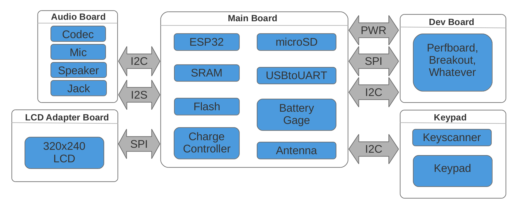
System Overview
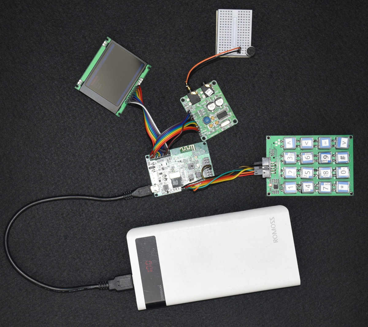
The WiPhone is composed of a few different functional areas as shown in the block diagram down at the bottom. For debugging, initially separate PCBs were used to because it's easier to swap out mistakes (and also to allow starting with an off the shelf keypad, LED, and audio breakout boards). We are moving out of this phase of the project, but wanted to document it here for reference.
Main Board: This is where most of the important bits are. ESP32 for the main processor and WiFi stack, memory, charging and power management, and a USB to UART adapter for firmware upload and external communication.
Audio Board: This breaks out all of the audio components, including a codec.
Keypad: Simple mechanical button pad with a keyscanner IC reporting button presses back to the processor over I2C.
LCD Adapter: Almost nothing going on here, just need to route the SPI connection back to the main board. Ideally this would be a parallel connection instead, but there just aren't enough free pins on the ESP32.
Dev Board: This is a prototyping area. Or whatever custom circuit you want area. Eventually the Dev Board would be the only one that remains outside the phone. An external connector would allow connecting or disconnecting whatever custom PCB you want to the phone. Similar to shields/capes/hats/Qwiic/Grove/Booster Packs/modules, but common sense indicates it requires inventing a new name. WiPhone Block Diagram