Daughter Board Design Guide
The WiPhone is expandable via spring loaded contacts on the back of the phone. The back panel can be replaced with a standard 1.6mm PCB, and controlled directly from the ESP32 processor through those contact points.
This design guide will give an overview of considerations for designing daughterboards. We provide an eagle footprint as well as some drawings that can be used to make custom daughterboards
Schematic Footprint
The schematic footprint of the daughterboard contains 2 header footprints for the pin connector nets and a table mapping the header numbers to the ESP32 pins and software pin names.
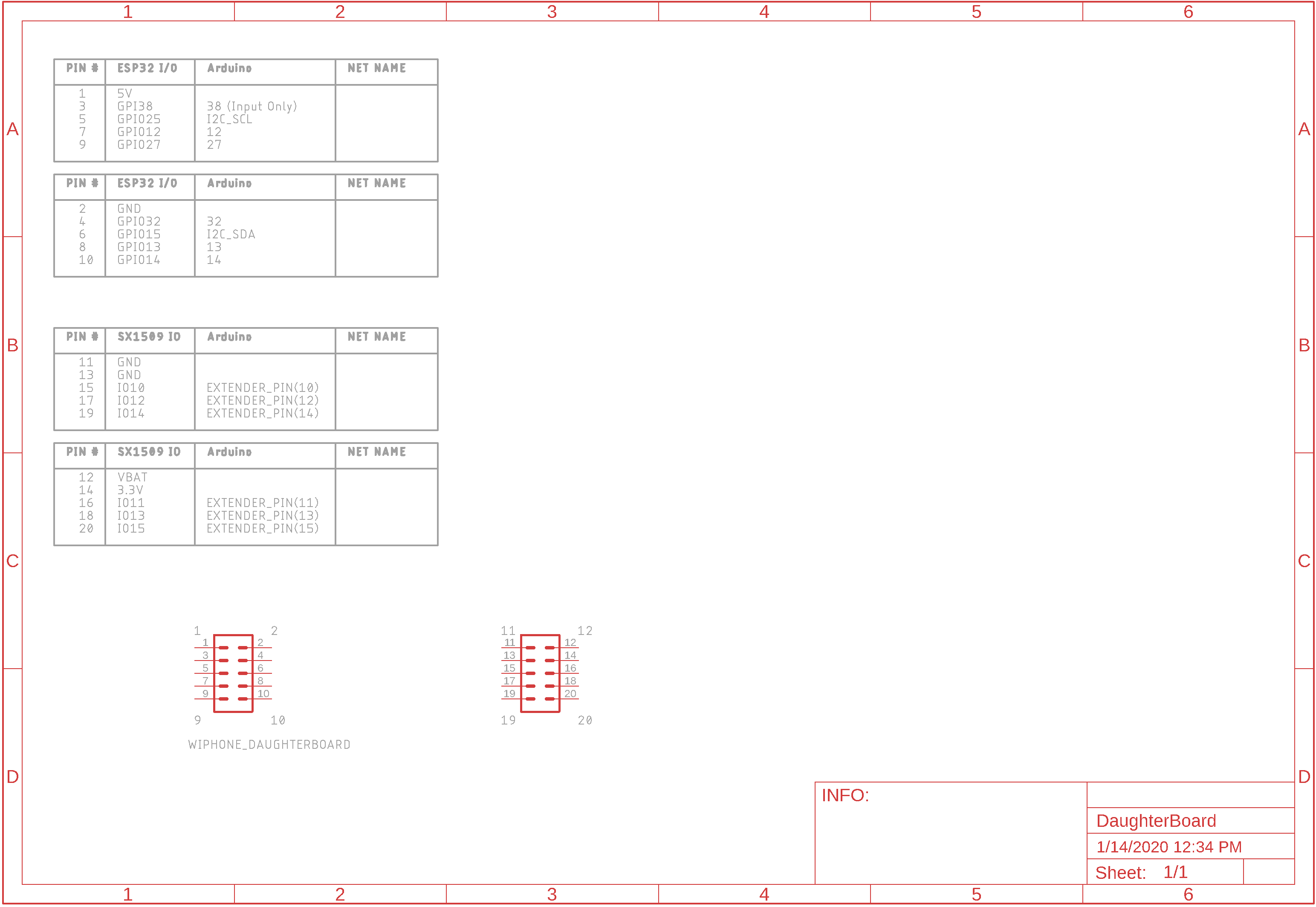
Daughter Board Schematic Symbol.
There is also an excel sheet Wiphone_IO_v2.5.xlsx with a more detailed description of each daughter board pin. You can download at https://wiphone.io/static/releases/pinout/Wiphone_IO_v2.5.xlsx
PCB Footprint
Various areas of the PCB have different height restrictions to avoid interference with nearby components. The drawing below shows an overview.
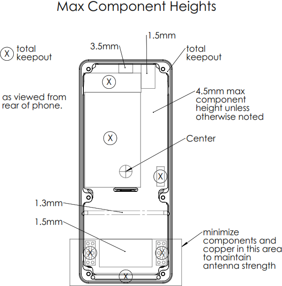
Daughter Board Keepouts.
Daughter Board Outline
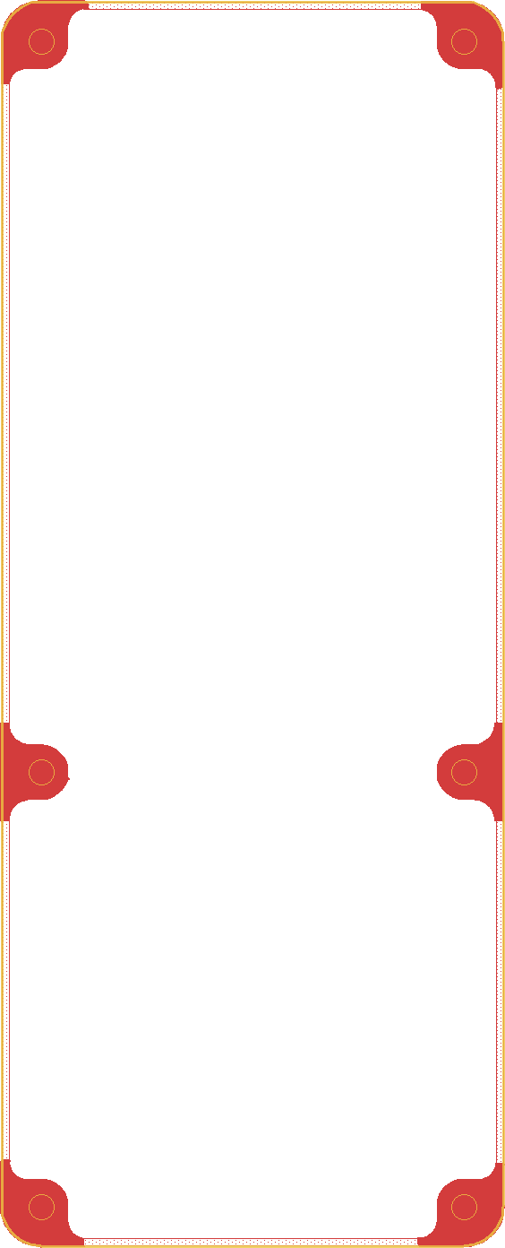
Daughter board dimensions are 117.5*47.5*1.6mm. There are six M2 screw holes, which may optionally be countersunk for appearance or minimal profile.
Ideally all components can be placed on the inside layer as this will protect them and have a better appearance. If this is not practical, components may be placed on the outside and left uncovered, or a plastic shell can be added.
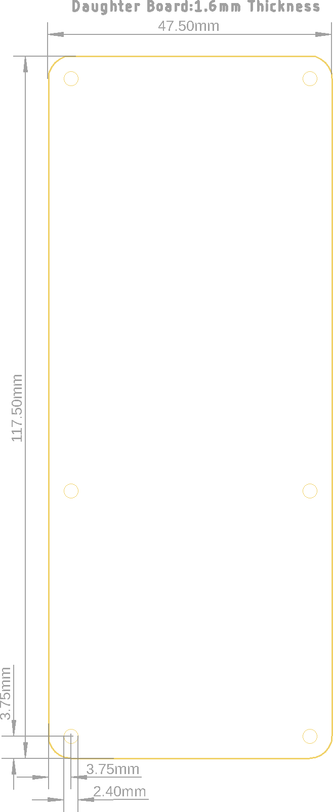
Daughter Board Dimensions.
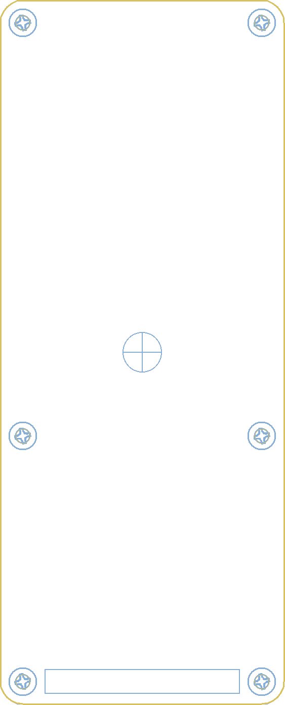
Bottom Component Keepout Area
When placing components on the inner side of daughter board, this keepout drawing can be used to prevent interference with components on the WiPhone mainboard as well as the phone frame.
The downloadable PCB footprint contains these same keepout zones.
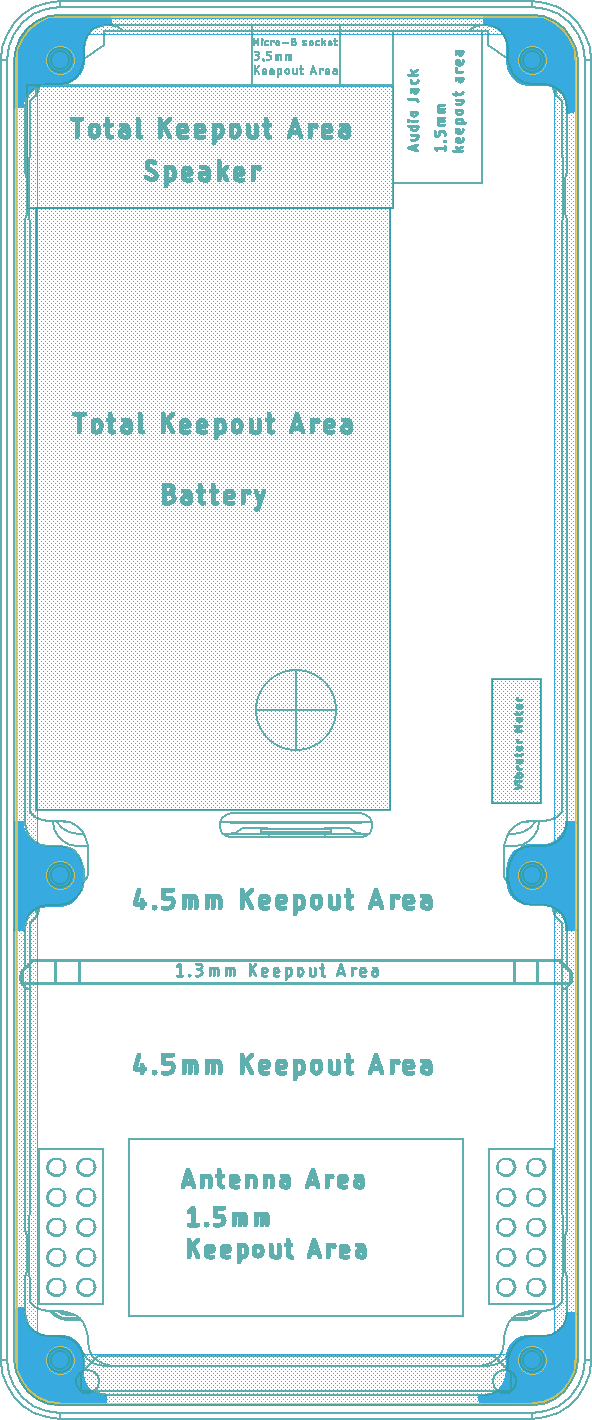
Daughter Board Bottom Keepouts.
Bottom Copper Restrict Area
The BottomKeepouts layer of the PCB footprint specifies the max allowable height of components in different areas. Some places shold be totally avoided, such as near the frame, battery, speaker and vibration motor. To keep WiFi signal strength, there is an additional area near the bottom of the phone that should be avoided (placing components or traces).
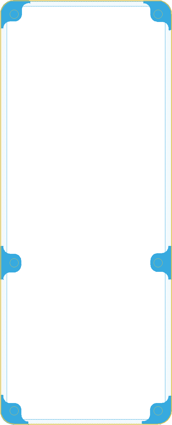
Daughter Board Bottom Restrict.
Pinout Labels
The bottom document bDocu layer contain a small daughter board pin description table labeling the pinout of the daughter board connectors.
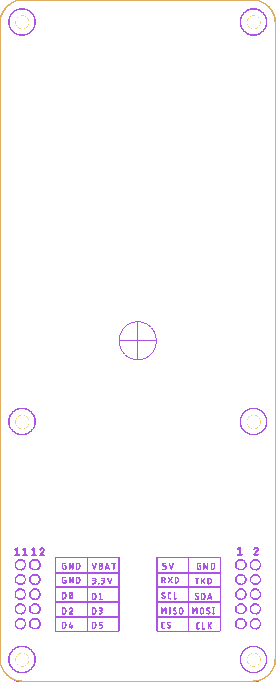
Daughter Board Pinout.
Bottom and Top Copper Keepout Area for Antenna
If your application requires good antenna strength, avoid placing components or traces in this area.
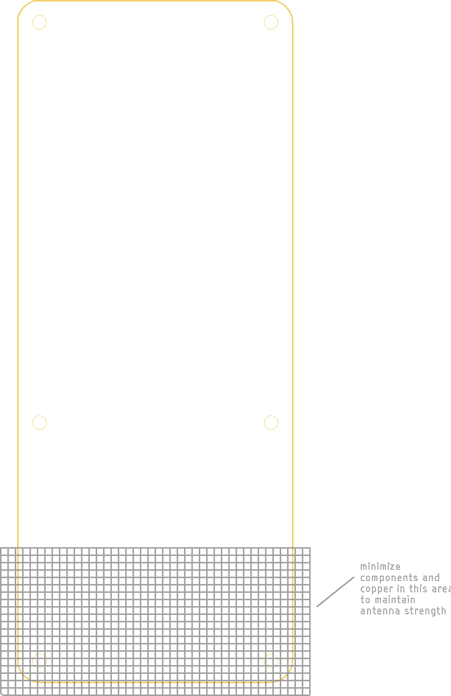
Daughter Board Copper Keepout Area for Antenna.
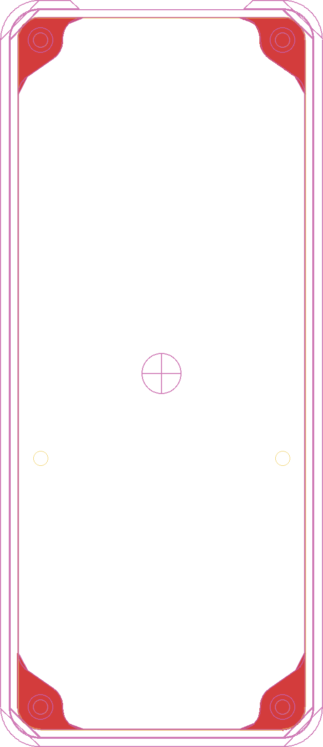
Top Components Keepout Area
If your board uses the hard shell back, avoid placing components in these areas of the top layer.
Daughter Board Top Keepouts.
Top Copper Restrict Area
These keepouts assume countersunk flathead M2s. If you are using a different type screw head, this keepout may need to be adjusted to prevent exposing copper.
Daughter Board Top Restrict.
Top Document Information
To standardize the look of daughter boards, the tDocu layer has a target rectangle for placing the daughterboard name.
Vector and proportional fonts tend to look ugly. If you are using Eagle to design your daughterboards you can improve the appearance by writing your board name in Board Name.svg and bring the artwork in as a monochrome bitmap image using a user script.
Daughter Board Top Document.